


 |
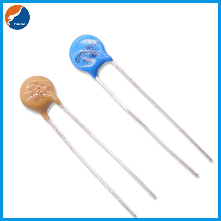
High Voltage ZOV MOV VDR Varistor 7D431K 7D471K 7D511K 7D561K
Product Details:
| Place of Origin: | China |
| Brand Name: | Tian Rui |
| Certification: | UL CSA VDE |
| Model Number: | 7D Varistors |
Payment & Shipping Terms:
| Minimum Order Quantity: | 1000PCS |
|---|---|
| Price: | Negotiable |
| Packaging Details: | PE Bag or Tape&Reel |
| Delivery Time: | 5-7 Days |
| Payment Terms: | D/P, T/T,Paypal, Western Union |
| Supply Ability: | 1000000PCS/Month |
|
Detail Information |
|||
| Disk: | Zinc Oxide | Coating: | Silicone |
|---|---|---|---|
| Lead: | Cp/Cu Wire | Electrode: | Silver |
| Epoxy Colour: | Green | Operating Temperature Range: | -40℃ ~ +85℃ |
| Storage Temperature Range: | -40℃ ~ +125℃ | Solder: | Sn:96.5%CU 0.5%Ag3.0% |
| Packing: | Bulk Or Tape | ||
| High Light: | 7D511K VDR Varistor,7D471K VDR Varistor,MOV 7D431K Varistor |
||
Product Description
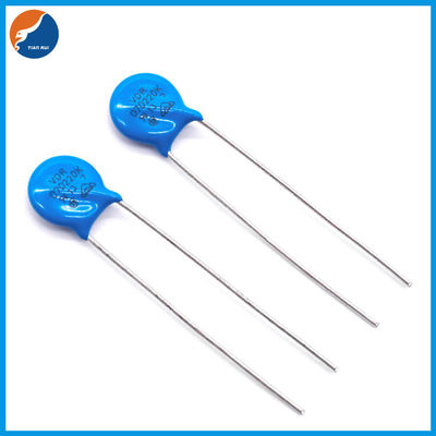
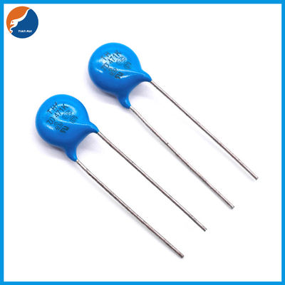
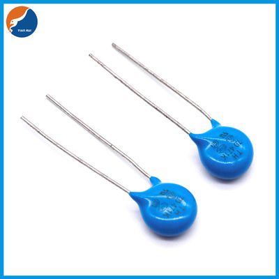
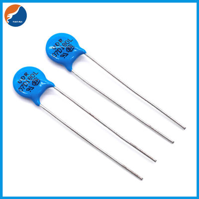
High Voltage 7D Series Pitch 7MM D Diamension VDR ZOV MOV Metal Zinc Oxide Varistor
![]()
DIMENSIONS
![]()
| Table1 | ||||||||||||||
| Unit:mm | ||||||||||||||
| Symbol | Dimension | |||||||||||||
| D(max.) | 9.0 | |||||||||||||
| H(max.) | 12.0 | |||||||||||||
| H0(max.) | 13.5 | |||||||||||||
| F(±0.8) | 5.0 | |||||||||||||
| T | Table2 | |||||||||||||
| d(±0.05) | 0.6 | |||||||||||||
| d1(±0.4) | 1.2 | |||||||||||||
| L(min.) | 20.0 | |||||||||||||
| L0(min.) | 15.0 | |||||||||||||
| Epoxy Colour : Green | ||||||||||||||
| Table2 | ||||||||||||||||||||
| Unit:mm | ||||||||||||||||||||
| Model | T | Model | T | |||||||||||||||||
| 180K | 2.03-3.35 | 271K | 2.57-4.21 | |||||||||||||||||
| 220K | 2.13-3.48 | 301K | 2.66-4.38 | |||||||||||||||||
| 270K | 2.23-3.67 | 331K | 2.76-4.56 | |||||||||||||||||
| 330K | 2.36-3.85 | 361K | 2.86-4.74 | |||||||||||||||||
| 390K | 2.31-3.66 | 391K | 2.95-4.92 | |||||||||||||||||
| 470K | 2.44-3.87 | 431K | 3.08-5.16 | |||||||||||||||||
| 560K | 2.58-4.10 | 471K | 3.21-5.39 | |||||||||||||||||
| 680K | 2.77-4.38 | 511K | 3.34-5.63 | |||||||||||||||||
| 820K | 2.18-3.39 | 561K | 3.50-5.93 | |||||||||||||||||
| 101K | 2.28-3.56 | 621K | 3.69-6.29 | |||||||||||||||||
| 121K | 2.40-3.76 | 681K | 3.89-6.64 | |||||||||||||||||
| 151K | 2.18-3.49 | 751K | 4.11-7.06 | |||||||||||||||||
| 181K | 2.28-3.67 | 781K | 4.21-7.24 | |||||||||||||||||
| 201K | 2.36-3.82 | 821K | 4.34-7.48 | |||||||||||||||||
| 221K | 2.41-3.91 | 911K | 4.63-8.01 | |||||||||||||||||
| 241K | 2.47-4.03 | |||||||||||||||||||
Electrical characteristics
| ZOV Part Number |
Maximum Allowable Voltage |
Varistor voltage | IR3 | @ | Clamping volatge | Maximum Peak Crurrent (8/20μs) |
Maximum Ebergt 10/1000μs |
Reted Power | Typical Capacitance (Reference) | |||||||||||||||||||||||
| Ac.rm s | DC | V1.0 mA | μA | VC | IP | Standard | High Surge | Standar d | High Surge | (w) | @1KHz | |||||||||||||||||||||
| (V) | (V) | (V) | (V) | (A) | (A) | (JOULE) | (pf) | |||||||||||||||||||||||||
| 07D180KP/Z | 11 | 14 | 18(15-21.6) | 50 | 10 | 36 | 2.5 | 250/125 *2 |
500/250 *2 |
0.9 | 2 | 0.02 | 2800 | |||||||||||||||||||
| 07D220KP/Z | 14 | 18 | 22(19.5-26) | 10 | 43 | 1.1 | 2.4 | 2300 | ||||||||||||||||||||||||
| 07D270KP/Z | 17 | 22 | 27(24-31) | 10 | 53 | 1.4 | 3 | 1800 | ||||||||||||||||||||||||
| 07D330KP/Z | 20 | 26 | 33(29.5-36.5) | 10 | 65 | 1.7 | 3.5 | 1500 | ||||||||||||||||||||||||
| 07D390KP/Z | 25 | 31 | 39(35-43) | 15 | 77 | 2.1 | 4 | 1300 | ||||||||||||||||||||||||
| 07D470KP/Z | 30 | 38 | 47(42-52) | 15 | 93 | 2.5 | 5 | 1100 | ||||||||||||||||||||||||
| 07D560KP/Z | 35 | 45 | 56(50-62) | 15 | 110 | 3.1 | 6 | 890 | ||||||||||||||||||||||||
| 07D680KP/Z | 40 | 56 | 68(61-75) | 15 | 135 | 3.6 | 7 | 740 | ||||||||||||||||||||||||
| 07D820KP/Z | 50 | 65 | 82(74-90) | 16 | 28 | 135 | 10 | 1200/60 0*2 |
1750/12 000*2 |
5.5 | 10 | 0.25 | 600 | |||||||||||||||||||
| 07D101KP/Z | 60 | 85 | 100(90-110) | 28 | 165 | 6.5 | 12 | 500 | ||||||||||||||||||||||||
| 07D121KP/Z | 75 | 100 | 120(108-132) | 28 | 200 | 7.8 | 13 | 420 | ||||||||||||||||||||||||
| 07D151KP/Z | 95 | 125 | 150(135-165) | 28 | 250 | 9.7 | 15 | 330 | ||||||||||||||||||||||||
| 07D181KP/Z | 115 | 150 | 180(162-198) | 38 | 300 | 11.7 | 16 | 280 | ||||||||||||||||||||||||
| 07D201KP/Z | 130 | 170 | 200(185-225) | 38 | 340 | 13 | 17 | 250 | ||||||||||||||||||||||||
| 07D221KP/Z | 140 | 180 | 220(198-242) | 38 | 360 | 14 | 19 | 230 | ||||||||||||||||||||||||
| 07D241KP/Z | 150 | 200 | 240(216-264) | 38 | 395 | 15 | 21 | 210 | ||||||||||||||||||||||||
| 07D271KP/Z | 175 | 225 | 270(243-297) | 38 | 455 | 18 | 24 | 185 | ||||||||||||||||||||||||
| 07D301KP/Z | 190 | 250 | 300(270-330) | 38 | 500 | 20 | 26 | 165 | ||||||||||||||||||||||||
| 07D331KP/Z | 210 | 275 | 330(297-363) | 38 | 550 | 23 | 28 | 150 | ||||||||||||||||||||||||
| 07D361KP/Z | 230 | 300 | 360(324-396) | 38 | 595 | 24 | 32 | 140 | ||||||||||||||||||||||||
| 07D391KP/Z | 250 | 320 | 390(351-429) | 38 | 650 | 26 | 35 | 130 | ||||||||||||||||||||||||
| 07D431KP/Z | 275 | 350 | 430(387-473) | 38 | 710 | 28 | 40 | 115 | ||||||||||||||||||||||||
| 07D471KP/Z | 300 | 385 | 470(423-517) | 38 | 775 | 29 | 42 | 105 | ||||||||||||||||||||||||
| 07D511KP/Z | 320 | 415 | 510(459-561) | 38 | 845 | 31 | 45 | 100 | ||||||||||||||||||||||||
| 07D561KP/Z | 350 | 460 | 560(504-616) | 38 | 925 | 35 | 49 | 90 | ||||||||||||||||||||||||
| 07D621KP/Z | 385 | 505 | 620(558-682) | 35 | 1025 | 38 | 55 | 80 | ||||||||||||||||||||||||
| 07D681KP/Z | 420 | 560 | 680(612-748) | 35 | 1120 | 42 | 60 | 75 | ||||||||||||||||||||||||
| 07D751KP/Z | 460 | 615 | 750(675-825) | 35 | 1240 | 45 | 64 | 70 | ||||||||||||||||||||||||
| 07D781KP/Z | 485 | 640 | 780(702-858) | 35 | 1290 | 48 | 69 | 65 | ||||||||||||||||||||||||
| 07D821KP/Z | 510 | 670 | 820(738-902) | 30 | 1355 | 52 | 73 | 60 | ||||||||||||||||||||||||
| 07D911KP/Z | 550 | 745 | 910(819-1001) | 30 | 1500 | 57 | 78 | 55 | ||||||||||||||||||||||||
ELETRICAL PARAMETER
| Max. Allowable Voltage | Reference p2* | At 1.0mA DC | ||||||||||||||||||||||||||
| Varistor Voltage(Test Time For 30ms) | V0.1mA □ V1mA ■ | |||||||||||||||||||||||||||
| Rated Wattage | ||||||||||||||||||||||||||||
| Max. Clamping Voltage | Test Current Waveform 8/20μs | |||||||||||||||||||||||||||
| Withstanding Surge Current | Test Current Waveform 8/20μs | |||||||||||||||||||||||||||
| Max. Energy | Test Current Waveform 10/1000μs | |||||||||||||||||||||||||||
| Typical Capacitance | @1KHz | |||||||||||||||||||||||||||
| Leakage Current | At 80% of Varistor Voltage | |||||||||||||||||||||||||||
| Nonlinear Exponent (α) | ||||||||||||||||||||||||||||
| Temperature Coefficient of Varistor Voltage | -0.05≤Tc≤0.05(% ℃) |
|||||||||||||||||||||||||||
| Impulse Life | ≦±10%(V1mA) | Test Current Waveform 8/20μs | ||||||||||||||||||||||||||
MATERIAL LIST
| Material Chart RoHs | Item | Composition | Manufacturer | ||||||||||||||||||||||||||
| Coating | Silicone | In line with the UL 94-V0 testing, meet the environmental requirements | |||||||||||||||||||||||||||
| Lead | Cp/Cu wire | Made in China, meet the environmental requirements | |||||||||||||||||||||||||||
| Electrode | Silver | Made in China, meet the environmental requirements | |||||||||||||||||||||||||||
| Disk | Zinc Oxide | Made in China, meet the environmental requirements | |||||||||||||||||||||||||||
| Solder | Sn:96.5%CU 0.5%Ag3.0% | Made in China, meet the environmental requirements | |||||||||||||||||||||||||||
MECHENICAL REQUIREMENTS
| Tensile of Terminations | No Outstanding Damage | 1.0Kgf; 10Sec. | |||||||||||||||||||||||||||
| Bending of Terminations | No Outstanding Damage | 0.5Kgf;90°,3 Times | |||||||||||||||||||||||||||
| Vibration | No Outstanding Damage | Freq:10-55hz;Amp:0.75mm,1Min . |
|||||||||||||||||||||||||||
| Solderability | Min. 95% of The Terminal Should Be Covered With Solder Uniformly |
Solder Temp:245±5℃ Immersed Time: ≤5Sec. | |||||||||||||||||||||||||||
| Resistance of soldering heat | △ V1mA/V1mA ≦±5% |
Solder Temp: 260±5℃ Immersed Time: 10±1Sec. | |||||||||||||||||||||||||||
ENVIRONMENTAL REQUIREMENTS
| High Temperature Storage | △ V1mA/V1mA ≦±5% |
Ambient Temp: 125±2℃ Duration:1000h | |||||||||||||||||||||||||||
| Low Temperature Storage | △ V1mA/V1mA ≦±5% |
Ambient Temp: -40±2℃ Duration:1000h | |||||||||||||||||||||||||||
| High Humidity Storage/Damp Heat | △ V1mA/V1mA ≦±5% |
Ambient Temp: 40±2℃ 90-95% R.H. Duration:1000h |
|||||||||||||||||||||||||||
| Temperature Cycle | △ V1mA/V1mA ≦±5% |
Step | Temperature (℃) |
Period (min) |
|||||||||||||||||||||||||
| 1 | -40±3 | 30 ±3 | |||||||||||||||||||||||||||
| 2 | Room Temp | 15 ±3 | |||||||||||||||||||||||||||
| 3 | 85±3 | 30 ±3 | |||||||||||||||||||||||||||
| 4 | Room Temp | 15 ±3 | |||||||||||||||||||||||||||
| High Temperature Load | △ V1mA/V1mA ≦±10% |
Ambient temp:85±2℃ Duration:1000h Load: MAX. Allowable Voltage | |||||||||||||||||||||||||||
| High Humidity Load | △ V1mA/V1mA ≦±10% |
Ambient Temp: 40±2℃ 90-95%R.H.Duration:1000H Load: MAX. Allowable Voltage |
|||||||||||||||||||||||||||
| Operating Temperature Range | -40℃ ~ +85℃ | ||||||||||||||||||||||||||||
| Storage Temperature Range | -40℃ ~ +125℃ | ||||||||||||||||||||||||||||
MARKING CODE
![]()
TAPING DIMENSIONS
| Symbol | Dimension (mm) | ||||||||||
| P | 12.7±1.0 | ||||||||||
| P0 | 12.7±0.3 | ||||||||||
| P1 | 3.85±0.7 | ||||||||||
| P2 | 6.35±1.3 | ||||||||||
| F | 5.0±0.8 | ||||||||||
| h | 0±2 | ||||||||||
| W | 18.0±1.0 | ||||||||||
| W0 | 12.0±1.0 | ||||||||||
| W1 | 9.0±0.5 | ||||||||||
| W2 | 3.0max | ||||||||||
| H | 20.0±2.0 | ||||||||||
| I | 1.0max | ||||||||||
| D0 | 4.0±0.2 | ||||||||||
| t | 0.6±0.3 | ||||||||||
| B | 32max | ||||||||||
QUANTITY
Basic Features
Protection characteristics. When the impact strength of the impact source does not exceed the specified value, the limiting voltage of the varistor is not allowed to exceed the impact resistance voltage that the protected object can withstand.
The varistor shall be able to work reliably for a specified length of time under specified ambient temperature and system voltage condftions; A large number of times it can reliably withstand a specified impact
Impact resistance, that is, the varistor itself should be able to withstand specified impact current, impact energy, and the average power when muliple shocks occur in succession.
After the intervention of the varistor in the system, in addition to the protection of the "safety valve", it will also bring in some additional effects, which is called the "secondary